Welcome to the official website of Semipower Technology Co., Ltd.

A high-tech enterprise integrating R & D, production and sales

R&D New Products with Advanced Technology Leading-edge Technology

Semipower Technology Co.,Ltd.

+86-13510282288

Semipower Technology Co., Ltd.-Technological Frontier Information-How to select COOLMOS during R&D of power supply?
Semipower News centres

Semipower Science and technology

Wechat Public Number

How to select COOLMOS during R&D of power supply?

Time:2019/10/22 14:18:07Number of visits:4216

What should be noticed when selecting COOLMOS during R&D of power supply? 

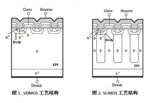
The structure difference between COOLMOS and VDMOS

In order to overcome the contradiction between on-resistance and breakdown voltage of traditional MOS, some people have proposed a new type of ideal device structure based on VDMOS, called super junction device or COOLMOS. The structure of COOLMOS is shown in Figure 2. COOLMOS is Consisted of alternating rows of P-type and N-type semiconductor thin layers. At off-state, due to the mutual compensation effect of the electric field in the depletion region of the P-type and N-type layers, the doping concentration of the P-type and N-type layers can be made very high without causing a decrease in the breakdown voltage of the device. When turned on, this high concentration of doping can significantly reduce its on-resistance. Because of this special structure, the performance of COOLMOS is better than traditional VDMOS.
For the conventional VDMOS device structure, if want to increase BV, we must start by reducing the EPI impurity concentration, but the epitaxial layer is a channel for forward current flow, and the EPI impurity concentration is reduced, the resistance must be increased, and Rdson will increase. Rdson directly determines the loss of the MOSFET cell. Therefore, for ordinary VDMOS, the two contradictions are irreconcilable, which is the limitation of conventional VDMOS.
But for COOLMOS, this contradiction is not so obvious. By setting a P-region that goes deep into the EPI, the BV is greatly improved without affecting the Rdson.


Advantages of COOLMOS in power supply:
1. Low on-state impedance and low on-state loss
2. Smaller package at the same power specification, which is conducive to the improvement of power density. 
3. The gate charge is small and the driving ability of the circuit is reduced.
4. Small capacitance, faster switching speed and low switching loss. 
Disadvantages:
1. Higher EMI
2. Gate oscillation
3. Poor ability for anti surge and voltage withstand
4. Higher Peak for drain-source voltage